5 Hours of Use from 5 Minutes of Charging for On-The-Go Productivity
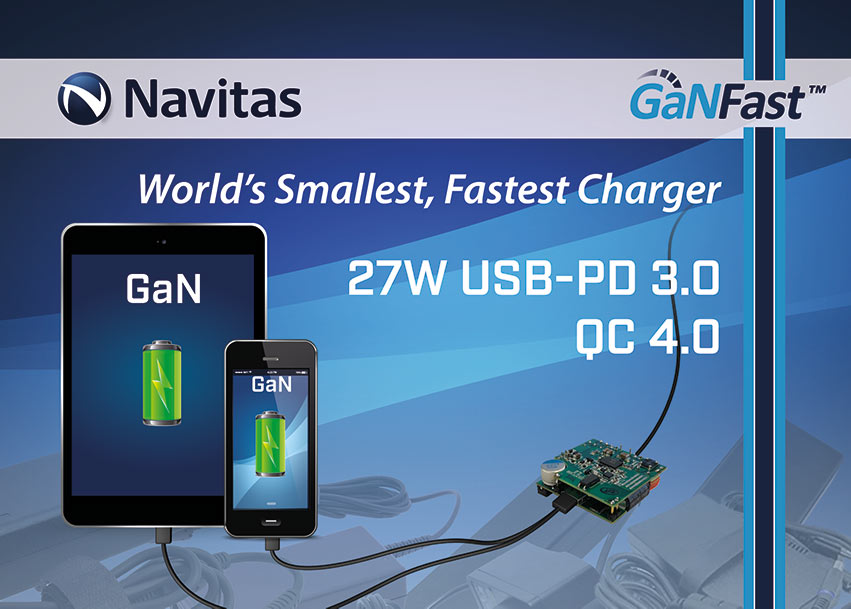
EL SEGUNDO, Calif.–(PRWeb)–Navitas Semiconductor announced today the world’s smallest, fastest charging mobile adapter enabled by GaNFast power ICs. The 27W design delivers 5x greater power than standard smartphone chargers and is 2x higher power density. With world-wide input voltage capability and a new Type C connector with USB-PD 3.0 and Qualcomm Quick Charge™ 4.0 features, this lightweight reference design delivers an extremely portable ‘go anywhere, charge anything’ solution.
“The 27W is another size and speed breakthrough for consumers enabled by GaNFast technology, and with Quick Charge 4.0 compliance, you can decrease the amount of time you spend tethered to an outlet giving your device ‘5 for 5’ — that’s 5 hours of battery life from 5 minutes of charging” said Stephen Oliver, Navitas’ vice president of sales & marketing. “Now that the high-frequency power eco-system of GaNFast power ICs, new controllers, new magnetics and soft-switching topologies has been established, we’ll see a wide-range of fast-charging, high density designs on the market.”
Using a Navitas’ high-speed, half-bridge GaNFast power IC in the advanced Active Clamp Flyback (ACF) topology, the 27W reference design measures only 39 x 37 x 16 mm (uncased) and achieves a world-record power density of 1.2 W/cc (19 W/in3) uncased and 0.7 W/cc (11 W/in3) assuming a 2.5 mm case thickness.
The 27W design (NVE039) will debut at the Navitas-sponsored Applied Power Electronics Conference (APEC) March 5th in San Antonio, Texas. It is available to qualified customers direct from Navitas at a price of $465 each, which includes a comprehensive user guide / test report with all schematic and layout design files, plus bill of material. For more information, contact +1 ThinkGaNIC (844-654-2642) or email [email protected].
Navitas Semiconductor Inc. is the world’s first and only GaN Power IC company, founded in 2013 and based in El Segundo, CA, USA. Navitas has a strong and growing team of power semiconductor industry experts with a combined 200 years of experience in materials, devices, applications, systems and marketing, plus a proven record of innovation with over 200 patents among its founders. The proprietary AllGaN™ process design kit monolithically integrates the highest performance GaN FETs with logic and analog circuits. Navitas GaN Power ICs enable smaller, higher energy efficient and lower cost power for mobile, consumer, enterprise and new energy markets. Over 30 Navitas patents are granted or pending.
Navitas Semiconductor, GaNFast and the Navitas logo are trademarks or registered trademarks of Navitas Semiconductor, Inc. All other brands, product names and marks are or may be trademarks or registered trademarks used to identify products or services of their respective owners.
Press Contact
Navitas Semiconductor Inc.
Stephen Oliver, +1 ThinkGaNIC (+1 844-654-2642)
VP, Sales & Marketing
[email protected]

Recent Comments